
Blocking & Non-Blocking
Blocking and Non Blocking :
In a software language like C or Python, code executes one line at a time, in sequence.
Python
# Software (Sequential)
x = 5
y = x # y is now 5
This is intuitive. Verilog can look similar, but hardware is different. In a real digital circuit, multiple things happen at the exact same time on a clock edge. All the flip-flops in your design trigger simultaneously. How do we model this parallelism? This is where the two types of assignments come in.
Blocking Assignment (=): Used for combinational logic. It executes in sequence within a block, just like software. The execution of the next line is "blocked" until the current one is complete.
Non-blocking Assignment (<=): Used for sequential logic. It models the parallel nature of hardware. All assignments are "scheduled" to happen at the end of the current simulation time step, without blocking the lines that follow.
The Classic Example: A Simple Shift Register
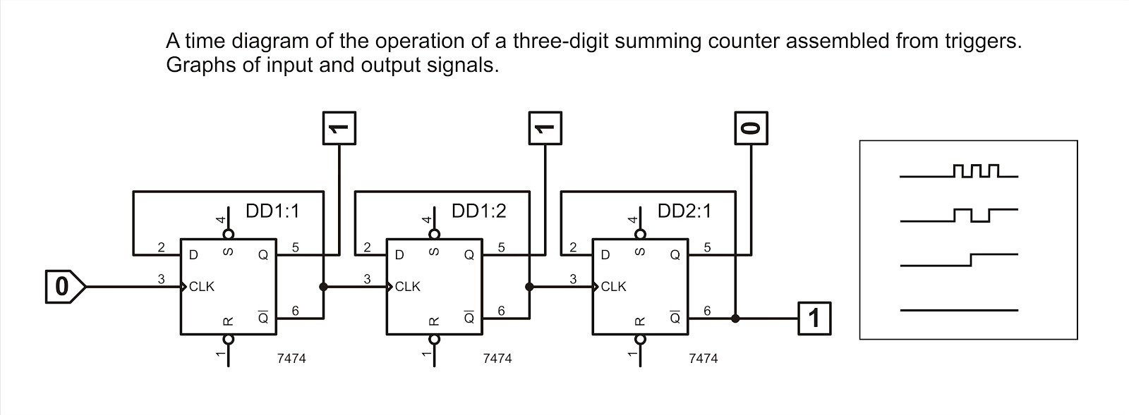
Let's design a 3-bit shift register. On each clock cycle, the value of din should move to q1, the old value of q1 should move to q2, and the old value of q2 should move to q3.
Attempt #1: The WRONG Way (Using Blocking =)
A beginner might write this, thinking it looks logical and sequential.
Verilog
// THIS IS INCORRECT HARDWARE - DO NOT USE FOR FLIP-FLOPS
module shift_register_blocking (
    input             clk,
    input             din,
    output reg [2:0]  q
);

    always @(posedge clk) begin
        q[0] = din;   // Blocking assignment
        q[1] = q[0];  // Blocking assignment
        q[2] = q[1];  // Blocking assignment
    end

endmodule
Why is this wrong? Let's trace the simulation at the first positive clock edge. Assume din = 1 and q = 000.
q[0] = din; executes. q[0] is immediately updated to 1. The internal value of q is now 001.
q[1] = q[0]; executes next. It reads the new value of q[0] (which is 1) and immediately updates q[1] to 1. The internal value of q is now 011.
q[2] = q[1]; executes last. It reads the new value of q[1] (which is 1) and immediately updates q[2] to 1. The internal value of q is now 111.
Result: In a single clock cycle, the input din has raced through the entire chain. This does not model a shift register! It models a simple wire where q[0], q[1], and q[2] are all equal to din. The simulation is misleading, and the synthesis tool will not produce three flip-flops.
Attempt #2: The CORRECT Way (Using Non-blocking <=)
Now let's write it the way it's done in industry.
Verilog
// THIS IS THE CORRECT WAY TO MODEL FLIP-FLOPS

module shift_register_nonblocking (
    input             clk,
    input             din,
    output reg [2:0]  q
);

    always @(posedge clk) begin
        q[0] <= din;   // Non-blocking assignment
        q[1] <= q[0];  // Non-blocking assignment
        q[2] <= q[1];  // Non-blocking assignment
    end

endmodule
Why is this correct? The Verilog simulator handles this always block differently. When the positive clock edge occurs, it does two things:
Evaluation Phase: It evaluates the Right-Hand Side (RHS) of every statement first, using the old values of the signals from before the clock edge.
It sees q[0] <= din; and reads the value of din (e.g., 1). It schedules q[0] to be updated to 1.
It sees q[1] <= q[0]; and reads the old value of q[0] (e.g., 0). It schedules q[1] to be updated to 0.
It sees q[2] <= q[1]; and reads the old value of q[1] (e.g., 0). It schedules q[2] to be updated to 0.
Update Phase: Now that all the RHS values have been read, the simulator performs the scheduled updates. q[0] becomes 1, q[1] becomes 0, and q[2] becomes 0.
Result: The value 1 has shifted into the first position, and the old values have moved one step to the right. This perfectly models the real-world behavior of three flip-flops all sampling their inputs on the same clock edge.
Top (Blocking): The waveform would show q[0], q[1], and q[2] all changing to match din at the same time after the clock edge.
Bottom (Non-Blocking): The waveform would show din's value appearing at q[0] after one clock cycle, at q[1] after two cycles, and at q[2] after three cycles. This is the correct shift register behavior.
The Golden Rules for RTL Design
To avoid issues and write professional, synthesizable code, follow these two rules religiously.
Rule 1: When modeling sequential logic (flip-flops, registers), always use non-blocking assignments (<=) inside an always @(posedge clk) block.
Rule 2: When modeling combinational logic (decoders, multiplexers), always use blocking assignments (=) inside an always @(*) block.
By separating your logic this way, you ensure that your simulation matches the behavior of the synthesized hardware, which is the ultimate goal of RTL design.