Latches
Latches
Latches are basic memory elements that are level-sensitive: their output follows inputs while an enable signal is active, and holds its state otherwise. Latches store one bit, and are often built from cross-coupled gates.
SR Latch
The SR latch is a type of latch which has two input lines designated as S and R. Where, S represents the Set input and R represents the Reset input. Thus, it is also known as Set-Reset Latch. SR flip flop can be constructed by 2 NOR Gates + 2 AND Gate OR by 4 NAND Gates.
The SR latch has two stable states namely Set state (S) and Reset state (R). The block diagram of the SR latch is shown in the following figure.
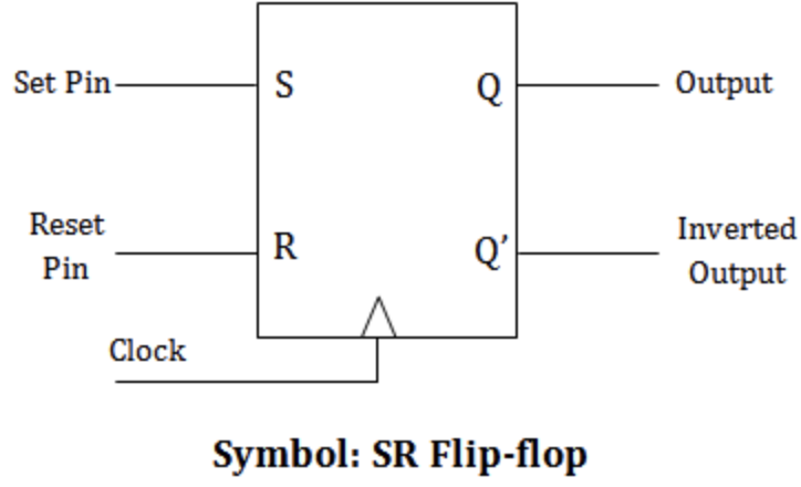
In the case of SR latch, the S input sets the output Q to 1 and Q' to 0. On the other hand, the R input sets the output Q to 0 and Q' to 1. In case, when both S and R inputs are high, the latch is said to be in forbidden state.
The complete operation of the SR latch for different input combinations is described in the following truth table −
Inputs | Outputs | Comment | ||
S | R | Q | Q' | |
0 | 0 | Q | Q' | No change |
0 | 1 | 0 | 1 | Reset state |
1 | 0 | 1 | 0 | Set state |
1 | 1 | X | X | Forbidden state |
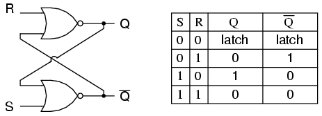
The SR latch can be implemented by connecting two NOR gates in a cross-coupled manner as shown in the following figure.
JK Latch
The JK latch is another type of latch which has two inputs namely, J and K. Here, the input J is similar to S input and the input K is similar to R input in an SR latch.
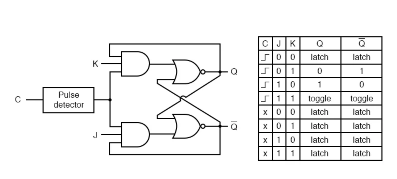
The operation of the JK latch is similar to that of the SR latch but it does not have the forbidden state. Instead, it has a toggle state in which the outputs Q and Q' swap their states when both inputs J and K are 1.
Therefor, the JK latch is mainly designed to overcome the problem of forbidden state in the SR latch.
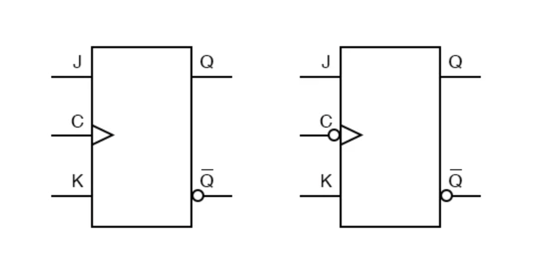
The block diagram of the JK latch is shown in the following figure −
The truth table given below describes the operation of the JK latch for different input combinations −
Inputs | Outputs | Comment | ||
J | K | Q | Q' | |
0 | 0 | Q | Q' | No change |
0 | 1 | 0 | 1 | Reset state |
1 | 0 | 1 | 0 | Set state |
1 | 1 | Q' | Q | Toggle state |
From this truth table, it is clear that the problem of forbidden state is addressed by implementing the toggle state.
The logic circuit of the JK latch consists of a combination of two NOR gates and two AND gates as shown in the following figure.
D Latch
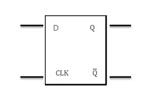
The D Latch, also known as Data latch or transparent latch, is a type of bistable multivibrator which has two input signals namely, D (Data) input and E (Enable) input.
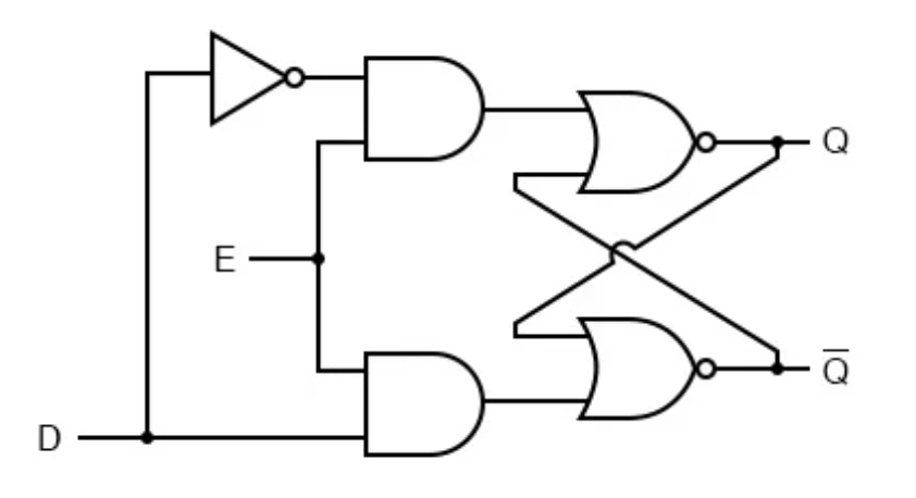
The output Q of the D latch is same as the input applied at the D input line as long as the E input is high. When the E input goes low, the output of the D latch is held as it is until the new input is applied to the D input.
The block diagram of the D latch is shown in the following figure.
The truth table given below explains the operation of the D latch −
Inputs | Outputs | Comment | ||
D | E | Q | Q' | |
0 | 0 | Q | Q' | No change |
0 | 1 | 0 | 1 | Reset state |
1 | 0 | Q | Q' | No change |
1 | 1 | 1 | 0 | Set state |
The logic circuit diagram of the D latch is depicted in the following figure −
T Latch
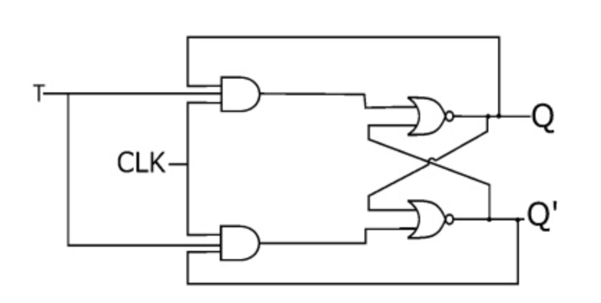
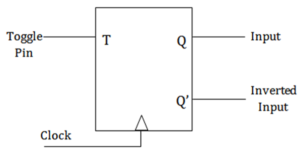
T latch is a type of latch that toggles its output state (Q) when a logic 1 is applied to its input line. Hence, it is also known as toggle latch.
The T latch is implemented by connecting the J and K inputs of the JK latch together as shown in the following block diagram.
The truth table describing the operation of the T latch is shown below −
Input | Present State | Next State | ||
T | Q | Q' | Q | Q' |
0 | 0 | 1 | 0 | 1 |
0 | 1 | 0 | 1 | 0 |
1 | 0 | 1 | 1 | 0 |
1 | 1 | 0 | 0 | 1 |
The logic circuit diagram of the T latch is shown in the following figure −